|
Electronic Components Datasheet Search |
|
|
Electronic Components Datasheet Search |
|
PIC16F7X7 Datasheet(PDF) 180 Page - Microchip Technology |
|
|
|||||||||||||||||||||||||||||
PIC16F7X7 Datasheet(HTML) 180 Page - Microchip Technology |
|
|
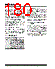
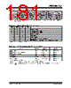
180 / 276 page  PIC16F7X7 DS30498C-page 178 2004 Microchip Technology Inc. 15.10.1 REFERENCE VOLTAGE SET POINT The internal reference voltage of the LVD module may be used by other internal circuitry (the Programmable Brown-out Reset). If these circuits are disabled (lower current consumption), the reference voltage circuit requires a time to become stable before a low-voltage condition can be reliably detected. This time is invariant of system clock speed. This start-up time is specified in electrical specification parameter #36. The low-voltage interrupt flag will not be enabled until a stable reference voltage is reached. Refer to the waveform in Figure 15-6. 15.10.2 CURRENT CONSUMPTION When the module is enabled, the LVD comparator and voltage divider are enabled and will consume static cur- rent. The voltage divider can be tapped from multiple places in the resistor array. Total current consumption, when enabled, is specified in electrical specification parameter #D022B. 15.11 Operation During Sleep When enabled, the LVD circuitry continues to operate during Sleep. If the device voltage crosses the trip point, the LVDIF bit will be set and the device will wake- up from Sleep. Device execution will continue from the interrupt vector address if interrupts have been globally enabled. 15.12 Effects of a Reset A device Reset forces all registers to their Reset state. This forces the LVD module to be turned off. 15.13 Time-out Sequence On power-up, the time-out sequence is as follows: the PWRT delay starts (if enabled) when a POR occurs; then, OST starts counting 1024 oscillator cycles when PWRT ends (LP, XT, HS); when the OST ends, the device comes out of Reset. If MCLR is kept low long enough, all delays will expire. Bringing MCLR high will begin execution immediately. This is useful for testing purposes or to synchronize more than one PIC16F7X7 device operating in parallel. Table 15-3 shows the Reset conditions for the Status, PCON and PC registers, while Table 15-4 shows the Reset conditions for all the registers. 15.14 Power Control/Status Register (PCON) The Power Control/Status register, PCON, has two bits to indicate the type of Reset that last occurred. Bit 0 is Brown-out Reset status bit, BOR. Bit BOR is unknown on a Power-on Reset. It must then be set by the user and checked on subsequent Resets to see if bit BOR cleared, indicating a Brown-out Reset occurred. When the Brown-out Reset is disabled, the state of the BOR bit is unpredictable. Bit 1 is Power-on Reset Status bit, POR. It is cleared on a Power-on Reset and unaffected otherwise. The user must set this bit following a Power-on Reset. Note: If the LVD is enabled and the BOR module is not enabled, the band gap will require a start-up time of no more than 50 µs before the band gap reference is stable. Before enabling the LVD interrupt, the user should ensure that the band gap reference voltage is stable by monitoring the IRVST bit in the LVDCON register. The LVD could cause erroneous interrupts before the band gap is stable. |
|
Link URL |
| Does ALLDATASHEET help your business so far? [ DONATE ] |
About Alldatasheet | Advertisement | Contact us | Privacy Policy | Link to Datasheet | Link Exchange | Manufacturer List All Rights Reserved©Alldatasheet.com |
| Russian : Alldatasheetru.com | Korean : Alldatasheet.co.kr | Spanish : Alldatasheet.es | French : Alldatasheet.fr | Italian : Alldatasheetit.com Portuguese : Alldatasheetpt.com | Polish : Alldatasheet.pl | Vietnamese : Alldatasheet.vn Indian : Alldatasheet.in | Mexican : Alldatasheet.com.mx | British : Alldatasheet.co.uk | New Zealand : Alldatasheet.co.nz |
|
Family Site : ic2ic.com |
icmetro.com |
 New Zealand ▼
 English
 Chinese
 German
 Japanese
 Russian
 Korean
 Spanish
 French
 Italian
 Portuguese
 Polish
 Vietnamese
 Indian
 Mexican
 British
 New Zealand