|
Electronic Components Datasheet Search |
|
|
Electronic Components Datasheet Search |
|
PIC16F7X7 Datasheet(PDF) 220 Page - Microchip Technology |
|
|
|||||||||||||||||||||||||||||
PIC16F7X7 Datasheet(HTML) 220 Page - Microchip Technology |
|
|
220 / 276 page 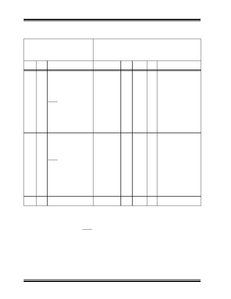 PIC16F7X7 DS30498C-page 218 2004 Microchip Technology Inc. 18.4 DC Characteristics: PIC16F737/747/767/777 (Industrial, Extended) PIC16LF737/747/767/777 (Industrial) DC CHARACTERISTICS Standard Operating Conditions (unless otherwise stated) Operating temperature -40°C ≤ TA ≤ +85°C for industrial -40°C ≤ TA ≤ +125°C for extended Operating voltage VDD range as described in Section 18.1 “DC Characteristics”. Param No. Sym Characteristic Min Typ† Max Units Conditions VIL Input Low Voltage I/O ports: D030 with TTL buffer VSS —0.15 VDD V For entire VDD range D030A VSS — 0.8V V 4.5V ≤ VDD ≤ 5.5V D031 with Schmitt Trigger buffer VSS — 0.2 VDD V D032 MCLR, OSC1 (in RC mode) VSS — 0.2 VDD V D033 OSC1 (in XT and LP modes) VSS —0.3V V (Note 1) OSC1 (in HS mode) VSS — 0.3 VDD V Ports RC3 and RC4: — D034 with Schmitt Trigger buffer VSS — 0.3 VDD V For entire VDD range D034A with SMBus -0.5 — 0.6 V For VDD = 4.5 to 5.5V VIH Input High Voltage I/O ports: — D040 with TTL buffer 2.0 — VDD V4.5V ≤ VDD ≤ 5.5V D040A 0.25 VDD + 0.8V — VDD V For entire VDD range D041 with Schmitt Trigger buffer 0.8 VDD —VDD V For entire VDD range D042 MCLR 0.8 VDD —VDD V D042A OSC1 (in XT and LP modes) 1.6V — VDD V (Note 1) OSC1 (in HS mode) 0.7 VDD —VDD V D043 OSC1 (in RC mode) 0.9 VDD —VDD V Ports RC3 and RC4: D044 with Schmitt Trigger buffer 0.7 VDD —VDD V For entire VDD range D044A with SMBus 1.4 — 5.5 V For VDD = 4.5 to 5.5V D070 IPURB PORTB Weak Pull-up Current 50 250 400 µAVDD = 5V, VPIN = VSS, -40°C TO +85°C * These parameters are characterized but not tested. † Data in “Typ” column is at 5V, 25°C unless otherwise stated. These parameters are for design guidance only and are not tested. Note 1: In RC oscillator configuration, the OSC1/CLKI pin is a Schmitt Trigger input. It is not recommended that the PIC16F7X7 be driven with external clock in RC mode. 2: The leakage current on the MCLR pin is strongly dependent on the applied voltage level. The specified levels represent normal operating conditions. Higher leakage current may be measured at different input voltages. 3: Negative current is defined as current sourced by the pin. |
|
Link URL |
| Does ALLDATASHEET help your business so far? [ DONATE ] |
About Alldatasheet | Advertisement | Contact us | Privacy Policy | Link to Datasheet | Link Exchange | Manufacturer List All Rights Reserved©Alldatasheet.com |
| Russian : Alldatasheetru.com | Korean : Alldatasheet.co.kr | Spanish : Alldatasheet.es | French : Alldatasheet.fr | Italian : Alldatasheetit.com Portuguese : Alldatasheetpt.com | Polish : Alldatasheet.pl | Vietnamese : Alldatasheet.vn Indian : Alldatasheet.in | Mexican : Alldatasheet.com.mx | British : Alldatasheet.co.uk | New Zealand : Alldatasheet.co.nz |
|
Family Site : ic2ic.com |
icmetro.com |
 New Zealand ▼
 English
 Chinese
 German
 Japanese
 Russian
 Korean
 Spanish
 French
 Italian
 Portuguese
 Polish
 Vietnamese
 Indian
 Mexican
 British
 New Zealand