|
Electronic Components Datasheet Search |
|
|
Electronic Components Datasheet Search |
|
PIC16F7X7 Datasheet(PDF) 148 Page - Microchip Technology |
|
|
|||||||||||||||||||||||||||||
PIC16F7X7 Datasheet(HTML) 148 Page - Microchip Technology |
|
|
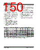
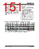
148 / 276 page  PIC16F7X7 DS30498C-page 146 2004 Microchip Technology Inc. 11.3.2 AUSART SYNCHRONOUS MASTER RECEPTION Once Synchronous mode is selected, reception is enabled by setting either enable bit, SREN (RCSTA<5>) or enable bit, CREN (RCSTA<4>). Data is sampled on the RC7/RX/DT pin on the falling edge of the clock. If enable bit SREN is set, then only a single word is received. If enable bit CREN is set, the recep- tion is continuous until CREN is cleared. If both bits are set, CREN takes precedence. After clocking the last bit, the received data in the Receive Shift Register (RSR) is transferred to the RCREG register (if it is empty). When the transfer is complete, interrupt flag bit, RCIF (PIR1<5>), is set. The actual interrupt can be enabled/ disabled by setting/clearing enable bit, RCIE (PIE1<5>). Flag bit RCIF is a read-only bit which is reset by the hardware. In this case, it is reset when the RCREG register has been read and is empty. The RCREG is a double-buffered register (i.e., it is a two- deep FIFO). It is possible for two bytes of data to be received and transferred to the RCREG FIFO and a third byte to begin shifting into the RSR register. On the clocking of the last bit of the third byte, if the RCREG register is still full, then Overrun Error bit, OERR (RCSTA<1>), is set. The word in the RSR will be lost. The RCREG register can be read twice to retrieve the two bytes in the FIFO. Bit OERR has to be cleared in software (by clearing bit CREN). If bit OERR is set, transfers from the RSR to the RCREG are inhibited, so it is essential to clear bit OERR if it is set. The ninth receive bit is buffered the same way as the receive data. Reading the RCREG register will load bit RX9D with a new value; therefore, it is essential for the user to read the RCSTA register before reading RCREG in order not to lose the old RX9D information. When setting up a Synchronous Master Reception: 1. Initialize the SPBRG register for the appropriate baud rate (see Section 11.1 “AUSART Baud Rate Generator (BRG)”). 2. Enable the synchronous master serial port by setting bits SYNC, SPEN and CSRC. 3. Ensure bits CREN and SREN are clear. 4. If interrupts are desired, then set enable bit RCIE. 5. If 9-bit reception is desired, then set bit RX9. 6. If a single reception is required, set bit SREN. For continuous reception, set bit CREN. 7. Interrupt flag bit RCIF will be set when reception is complete and an interrupt will be generated if enable bit RCIE was set. 8. Read the RCSTA register to get the ninth bit (if enabled) and determine if any error occurred during reception. 9. Read the 8-bit received data by reading the RCREG register. 10. If any error occurred, clear the error by clearing bit CREN. 11. If using interrupts, ensure that GIE and PEIE (bits 7 and 6) of the INTCON register are set. TABLE 11-11: REGISTERS ASSOCIATED WITH SYNCHRONOUS MASTER RECEPTION Address Name Bit 7 Bit 6 Bit 5 Bit 4 Bit 3 Bit 2 Bit 1 Bit 0 Value on: POR, BOR Value on all other Resets 0Bh, 8Bh, 10Bh,18Bh INTCON GIE PEIE TMR0IE INT0IE RBIE TMR0IF INT0IF RBIF 0000 000x 0000 000u 0Ch PIR1 PSPIF(1) ADIF RCIF TXIF SSPIF CCP1IF TMR2IF TMR1IF 0000 0000 0000 0000 18h RCSTA SPEN RX9 SREN CREN ADDEN FERR OERR RX9D 0000 000x 0000 000x 1Ah RCREG AUSART Receive Register 0000 0000 0000 0000 8Ch PIE1 PSPIE(1) ADIE RCIE TXIE SSPIE CCP1IE TMR2IE TMR1IE 0000 0000 0000 0000 98h TXSTA CSRC TX9 TXEN SYNC — BRGH TRMT TX9D 0000 -010 0000 -010 99h SPBRG Baud Rate Generator Register 0000 0000 0000 0000 Legend: x = unknown, — = unimplemented, read as ‘0’. Shaded cells are not used for synchronous master reception. Note 1: Bits PSPIE and PSPIF are reserved on 28-pin devices; always maintain these bits clear. |
|
Link URL |
| Does ALLDATASHEET help your business so far? [ DONATE ] |
About Alldatasheet | Advertisement | Contact us | Privacy Policy | Link to Datasheet | Link Exchange | Manufacturer List All Rights Reserved©Alldatasheet.com |
| Russian : Alldatasheetru.com | Korean : Alldatasheet.co.kr | Spanish : Alldatasheet.es | French : Alldatasheet.fr | Italian : Alldatasheetit.com Portuguese : Alldatasheetpt.com | Polish : Alldatasheet.pl | Vietnamese : Alldatasheet.vn Indian : Alldatasheet.in | Mexican : Alldatasheet.com.mx | British : Alldatasheet.co.uk | New Zealand : Alldatasheet.co.nz |
|
Family Site : ic2ic.com |
icmetro.com |
 New Zealand ▼
 English
 Chinese
 German
 Japanese
 Russian
 Korean
 Spanish
 French
 Italian
 Portuguese
 Polish
 Vietnamese
 Indian
 Mexican
 British
 New Zealand