|
Electronic Components Datasheet Search |
|
|
Electronic Components Datasheet Search |
|
PIC16F7X7 Datasheet(PDF) 160 Page - Microchip Technology |
|
|
|||||||||||||||||||||||||||||
PIC16F7X7 Datasheet(HTML) 160 Page - Microchip Technology |
|
|
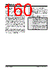
160 / 276 page  PIC16F7X7 DS30498C-page 158 2004 Microchip Technology Inc. 12.4 Operation in Power-Managed Modes The selection of the automatic acquisition time and A/D conversion clock is determined in part by the clock source and frequency while in a power-managed mode. If the A/D is expected to operate while the device is in a power-managed mode, the ACQT2:ACQT0 (ADCON2<5:3>) and ADCS2:ADCS0 (ADCON1<6>, ADCON0<7:6>) bits should be updated in accordance with the power-managed mode clock that will be used. After the power-managed mode is entered (either of the power-managed Run modes), an A/D acquisition or conversion may be started. Once an acquisition or conversion is started, the device should continue to be clocked by the same power-managed mode clock source until the conversion has been completed. If the power-managed mode clock frequency is less than 1 MHz, the A/D RC clock source should be selected. Operation in Sleep mode requires the A/D RC clock to be selected. If bits ACQT2:ACQT0 are set to ‘000’ and a conversion is started, the conversion will be delayed one instruction cycle to allow execution of the SLEEP instruction and entry to Sleep mode. 12.5 Configuring Analog Port Pins The ADCON1, TRISA, TRISB and TRISE registers control the operation of the A/D port pins. The port pins that are desired as analog inputs must have their corresponding TRIS bits set (input). If the TRIS bit is cleared (output), the digital output level (VOH or VOL) will be converted. The A/D operation is independent of the state of the CHS2:CHS0 bits and the TRIS bits. Note 1: When reading the Port register, all pins configured as analog input channels will read as cleared (a low level). Pins con- figured as digital inputs will convert an analog input. Analog levels on a digitally configured input will not affect the conversion accuracy. 2: Analog levels on any pin that is defined as a digital input, but not as an analog input, may cause the digital input buffer to consume current that is out of the device’s specification. |
|
Link URL |
| Does ALLDATASHEET help your business so far? [ DONATE ] |
About Alldatasheet | Advertisement | Contact us | Privacy Policy | Link to Datasheet | Link Exchange | Manufacturer List All Rights Reserved©Alldatasheet.com |
| Russian : Alldatasheetru.com | Korean : Alldatasheet.co.kr | Spanish : Alldatasheet.es | French : Alldatasheet.fr | Italian : Alldatasheetit.com Portuguese : Alldatasheetpt.com | Polish : Alldatasheet.pl | Vietnamese : Alldatasheet.vn Indian : Alldatasheet.in | Mexican : Alldatasheet.com.mx | British : Alldatasheet.co.uk | New Zealand : Alldatasheet.co.nz |
|
Family Site : ic2ic.com |
icmetro.com |
 New Zealand ▼
 English
 Chinese
 German
 Japanese
 Russian
 Korean
 Spanish
 French
 Italian
 Portuguese
 Polish
 Vietnamese
 Indian
 Mexican
 British
 New Zealand