|
Electronic Components Datasheet Search |
|
|
Electronic Components Datasheet Search |
|
PIC16F7X7 Datasheet(PDF) 238 Page - Microchip Technology |
|
|
|||||||||||||||||||||||||||||
PIC16F7X7 Datasheet(HTML) 238 Page - Microchip Technology |
|
|
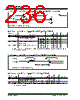
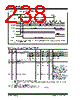
238 / 276 page 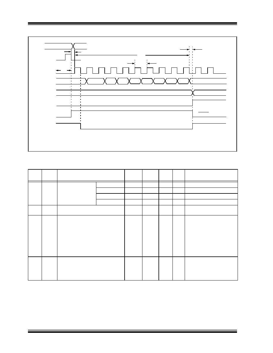 PIC16F7X7 DS30498C-page 236 2004 Microchip Technology Inc. FIGURE 18-20: A/D CONVERSION TIMING TABLE 18-16: A/D CONVERSION REQUIREMENTS 131 130 132 BSF ADCON0, GO Q4 A/D CLK A/D DATA ADRES ADIF GO SAMPLE OLD_DATA Sampling Stopped DONE NEW_DATA (TOSC/2)(1) 98 7 2 1 0 Note: If the A/D clock source is selected as RC, a time of TCY is added before the A/D clock starts. This allows the SLEEP instruction to be executed. 1 TCY . . . . . . Param No. Symbol Characteristic Min Typ† Max Units Conditions 130 TAD A/D Clock Period PIC16F7X7 1.6 — — µsTOSC based, VREF ≥ 3.0V PIC16LF7X7 3.0 — — µsTOSC based, VREF ≥ 2.0V PIC16F7X7 2.0 4.0 6.0 µs A/D RC mode PIC16LF7X7 3.0 6.0 9.0 µs A/D RC mode 131 TCNV Conversion Time (not including S/H time) (Note 1) —12 TAD 132 TACQ Acquisition Time (Note 2) 10* 40 — — — µs µs The minimum time is the amplifier settling time. This may be used if the “new” input voltage has not changed by more than 1 LSb (i.e., 5.0 mV @ 5.12V) from the last sampled voltage (as stated on CHOLD). 134 TGO Q4 to A/D Clock Start — TOSC/2 § — — If the A/D clock source is selected as RC, a time of TCY is added before the A/D clock starts. This allows the SLEEP instruction to be executed. * These parameters are characterized but not tested. † Data in “Typ” column is at 5V, 25°C unless otherwise stated. These parameters are for design guidance only and are not tested. § This specification ensured by design. Note 1: ADRES register may be read on the following TCY cycle. 2: See Section 12.1 “A/D Acquisition Requirements” for minimum conditions. |
|
Link URL |
| Does ALLDATASHEET help your business so far? [ DONATE ] |
About Alldatasheet | Advertisement | Contact us | Privacy Policy | Link to Datasheet | Link Exchange | Manufacturer List All Rights Reserved©Alldatasheet.com |
| Russian : Alldatasheetru.com | Korean : Alldatasheet.co.kr | Spanish : Alldatasheet.es | French : Alldatasheet.fr | Italian : Alldatasheetit.com Portuguese : Alldatasheetpt.com | Polish : Alldatasheet.pl | Vietnamese : Alldatasheet.vn Indian : Alldatasheet.in | Mexican : Alldatasheet.com.mx | British : Alldatasheet.co.uk | New Zealand : Alldatasheet.co.nz |
|
Family Site : ic2ic.com |
icmetro.com |
 New Zealand ▼
 English
 Chinese
 German
 Japanese
 Russian
 Korean
 Spanish
 French
 Italian
 Portuguese
 Polish
 Vietnamese
 Indian
 Mexican
 British
 New Zealand