|
Electronic Components Datasheet Search |
|
|
Electronic Components Datasheet Search |
|
PIC16F7X7 Datasheet(PDF) 172 Page - Microchip Technology |
|
|
|||||||||||||||||||||||||||||
PIC16F7X7 Datasheet(HTML) 172 Page - Microchip Technology |
|
|
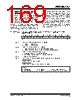
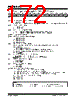
172 / 276 page  PIC16F7X7 DS30498C-page 170 2004 Microchip Technology Inc. REGISTER 15-1: CONFIGURATION WORD REGISTER 1 (ADDRESS 2007h) R/P-1 R/P-1 R/P-1 U-1 U-1 R/P-1 R/P-1 R/P-1 R/P-1 R/P-1 R/P-1 R/P-1 R/P-1 R/P-1 CP CCPMX DEBUG — — BORV1 BORV0 BOREN MCLRE FOSC2 PWRTEN WDTEN FOSC1 FOSC0 bit 13 bit 0 bit 13 CP: Flash Program Memory Code Protection bits 1 = Code protection off 0 = 0000h to 1FFFh code-protected for PIC16F767/777 and 0000h to 0FFFh for PIC16F737/747 (all protected) bit 12 CCPMX: CCP2 Multiplex bit 1 = CCP2 is on RC1 0 = CCP2 is on RB3 bit 11 DEBUG: In-Circuit Debugger Mode bit 1 = In-Circuit Debugger disabled, RB6 and RB7 are general purpose I/O pins 0 = In-Circuit Debugger enabled, RB6 and RB7 are dedicated to the debugger bit 10-9 Unimplemented: Read as ‘1’ bit 8-7 BORV<1:0>: Brown-out Reset Voltage bits 11 = VBOR set to 2.0V 10 = VBOR set to 2.7V 01 = VBOR set to 4.2V 00 = VBOR set to 4.5V bit 6 BOREN: Brown-out Reset Enable bit BOREN combines with BORSEN to control when BOR is enabled and how it is controlled. BOREN:BORSEN: 11 = BOR enabled and always on 10 = BOR enabled during operation and disabled during Sleep by hardware 01 = BOR controlled by software bit SBOREN – refer to Register 2-8 (PCON<2>) 00 = BOR disabled bit 5 MCLRE: MCLR/VPP/RE3 Pin Function Select bit 1 = MCLR/VPP/RE3 pin function is MCLR 0 = MCLR/VPP/RE3 pin function is digital input only, MCLR gated to ‘1’ bit 3 PWRTEN: Power-up Timer Enable bit 1 = PWRT disabled 0 = PWRT enabled bit 2 WDTEN: Watchdog Timer Enable bit 1 = WDT enabled 0 = WDT disabled bit 4, 1-0 FOSC2:FOSC0: Oscillator Selection bits 111 = EXTRC oscillator; CLKO function on OSC2/CLKO/RA6 110 = EXTRC oscillator; port I/O function on OSC2/CLKO/RA6 101 = INTRC oscillator; CLKO function on OSC2/CLKO/RA6 and port I/O function on OSC1/CLKI/RA7 100 = INTRC oscillator; port I/O function on OSC1/CLKI/RA7 and OSC2/CLKO/RA6 011 = EXTCLK; port I/O function on OSC2/CLKO/RA6 010 = HS oscillator 001 = XT oscillator 000 = LP oscillator Legend: R = Readable bit W = Writable bit U = Unimplemented bit, read as ‘0’ -n = Value at POR ‘1’ = Bit is set ‘0’ = Bit is cleared x = Bit is unknown |
|
Link URL |
| Does ALLDATASHEET help your business so far? [ DONATE ] |
About Alldatasheet | Advertisement | Contact us | Privacy Policy | Link to Datasheet | Link Exchange | Manufacturer List All Rights Reserved©Alldatasheet.com |
| Russian : Alldatasheetru.com | Korean : Alldatasheet.co.kr | Spanish : Alldatasheet.es | French : Alldatasheet.fr | Italian : Alldatasheetit.com Portuguese : Alldatasheetpt.com | Polish : Alldatasheet.pl | Vietnamese : Alldatasheet.vn Indian : Alldatasheet.in | Mexican : Alldatasheet.com.mx | British : Alldatasheet.co.uk | New Zealand : Alldatasheet.co.nz |
|
Family Site : ic2ic.com |
icmetro.com |
 New Zealand ▼
 English
 Chinese
 German
 Japanese
 Russian
 Korean
 Spanish
 French
 Italian
 Portuguese
 Polish
 Vietnamese
 Indian
 Mexican
 British
 New Zealand