|
Electronic Components Datasheet Search |
|
|
Electronic Components Datasheet Search |
|
PIC16F7X7 Datasheet(PDF) 191 Page - Microchip Technology |
|
|
|||||||||||||||||||||||||||||
PIC16F7X7 Datasheet(HTML) 191 Page - Microchip Technology |
|
|
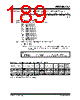
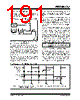
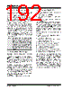
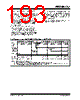
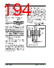
191 / 276 page  2004 Microchip Technology Inc. DS30498C-page 189 PIC16F7X7 15.17.4 FAIL-SAFE OPTION The Fail-Safe Clock Monitor (FSCM) is designed to allow the device to continue to operate even in the event of an oscillator failure. FIGURE 15-14: FSCM BLOCK DIAGRAM The FSCM function is enabled by setting the FCMEN bit in Configuration Word Register 2. In the event of an oscillator failure, the FSCM will generate an oscillator fail interrupt and will switch the system clock over to the internal oscillator. The system will continue to come from the internal oscillator until the Fail-Safe condition is exited. The Fail-Safe condition is exited with either a Reset, the execution of a SLEEP instruction or a write to the SCS bits of a different value. The frequency of the internal oscillator will depend upon the value contained in the IRCF bits. Another clock source can be selected via the IRCF and the SCS bits of the OSCCON register. The FSCM sample clock is generated by dividing the INTRC clock by 64. This will allow enough time between FSCM sample clocks for a system clock edge to occur. On the rising edge of the postscaled clock, the monitoring latch (CM = 0) will be cleared. On a falling edge of the primary or secondary system clock, the monitoring latch will be set (CM = 1). In the event that a falling edge of the postscaled clock occurs and the monitoring latch is not set, a clock failure has been detected. While in Fail-Safe mode, a Reset will exit the Fail-Safe condition. If the primary clock source is configured for a crystal, the OST timer will wait for the 1024 clock cycles for the OST time-out and the device will continue running from the internal oscillator until the OST is complete. A SLEEP instruction, or a write to the SCS bits (where SCS bits do not = 00), can be performed to put the device into a low-power mode. If Reset occurs while in Fail-Safe mode and the primary clock source is EC or RC, then the device will immediately switch back to EC or RC mode. 15.17.4.1 Fail-Safe in Low-Power Mode A change of SCS<1:0> or the SLEEP instruction will end the Fail-Safe condition. The system clock will default to the source selected by the SCS bits, which is either T1OSC, INTRC or none (Sleep mode). How- ever, the FSCM will continue to monitor the system clock. If the secondary clock fails, the device will immediately switch to the internal oscillator clock. If OSFIE is set, an interrupt will be generated. FIGURE 15-15: FSCM TIMING DIAGRAM Peripheral INTRC ÷ 64 S C Q 31.25 kHz (32 µs) 488 Hz (2.048 ms) Clock Monitor Latch (CM) (edge-triggered) Clock Failure Detected Oscillator Clock Q Note: Two-Speed Start-up is automatically enabled when the Fail-Safe option is enabled. OSCFIF CM Output System Clock Output Sample Clock Failure Detected Oscillator Failure Note: The system clock is normally at a much higher frequency than the sample clock. The relative frequencies in this example have been chosen for clarity. (Q) CM Test CM Test CM Test (488 Hz) |
|
Link URL |
| Does ALLDATASHEET help your business so far? [ DONATE ] |
About Alldatasheet | Advertisement | Contact us | Privacy Policy | Link to Datasheet | Link Exchange | Manufacturer List All Rights Reserved©Alldatasheet.com |
| Russian : Alldatasheetru.com | Korean : Alldatasheet.co.kr | Spanish : Alldatasheet.es | French : Alldatasheet.fr | Italian : Alldatasheetit.com Portuguese : Alldatasheetpt.com | Polish : Alldatasheet.pl | Vietnamese : Alldatasheet.vn Indian : Alldatasheet.in | Mexican : Alldatasheet.com.mx | British : Alldatasheet.co.uk | New Zealand : Alldatasheet.co.nz |
|
Family Site : ic2ic.com |
icmetro.com |
 New Zealand ▼
 English
 Chinese
 German
 Japanese
 Russian
 Korean
 Spanish
 French
 Italian
 Portuguese
 Polish
 Vietnamese
 Indian
 Mexican
 British
 New Zealand