|
Electronic Components Datasheet Search |
|
|
Electronic Components Datasheet Search |
|
ELANSC520 Datasheet(PDF) 27 Page - Advanced Micro Devices |
|
|
|||||||||||||||||||||||||||||
ELANSC520 Datasheet(HTML) 27 Page - Advanced Micro Devices |
|
|
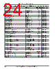
27 / 440 page  Configuration Register Overview Élan™SC520 Microcontroller Register Set Manual 1-7 1.2 DIRECT-MAPPED I/O REGISTERS The direct-mapped I/O registers include the Configuration Base Address (CBAR) register and PC/AT-compatible peripheral registers, such as the programmable interval timer (PIT), programmable interrupt controller (PIC), direct memory access (DMA) controller, the real- time clock (RTC) index and data registers, the PCI configuration address and data registers, two universal asynchronous receive/transmit (UART) devices, and miscellaneous control registers defined for compatibility. (The microcontroller’s third PIC and the CBAR register are not found in PC/AT-compatible systems.) Table 1-2 lists all of the direct-mapped I/O registers in the ÉlanSC520 microcontroller. GP-DMA Channel 6 Next Address High GPDMANXTADDH6 DAAh page 11-31 GP-DMA Channel 7 Next Address Low GPDMANXTADDL7 DACh page 11-32 GP-DMA Channel 7 Next Address High GPDMANXTADDH7 DAEh page 11-33 GP-DMA Channel 3 Next Transfer Count Low GPDMANXTTCL3 DB0h page 11-34 GP-DMA Channel 3 Next Transfer Count High GPDMANXTTCH3 DB2h page 11-35 GP-DMA Channel 5 Next Transfer Count Low GPDMANXTTCL5 DB4h page 11-36 GP-DMA Channel 5 Next Transfer Count High GPDMANXTTCH5 DB6h page 11-37 GP-DMA Channel 6 Next Transfer Count Low GPDMANXTTCL6 DB8h page 11-38 GP-DMA Channel 6 Next Transfer Count High GPDMANXTTCH6 DBAh page 11-39 GP-DMA Channel 7 Next Transfer Count Low GPDMANXTTCL7 DBCh page 11-40 GP-DMA Channel 7 Next Transfer Count High GPDMANXTTCH7 DBEh page 11-41 Table 1-2 Direct-Mapped I/O Registers Register Name Mnemonic I/O Address Page Number Slave DMA 0000–000Fh Slave DMA Channel 0 Memory Address GPDMA0MAR 0000h page 11-42 Slave DMA Channel 0 Transfer Count GPDMA0TC 0001h page 11-43 Slave DMA Channel 1 Memory Address GPDMA1MAR 0002h page 11-44 Slave DMA Channel 1 Transfer Count GPDMA1TC 0003h page 11-45 Slave DMA Channel 2 Memory Address GPDMA2MAR 0004h page 11-46 Slave DMA Channel 2 Transfer Count GPDMA2TC 0005h page 11-47 Slave DMA Channel 3 Memory Address GPDMA3MAR 0006h page 11-48 Slave DMA Channel 3 Transfer Count GPDMA3TC 0007h page 11-49 Slave DMA Channel 0–3 Status SLDMASTA 0008h page 11-50 Slave DMA Channel 0–3 Control SLDMACTL 0008h page 11-51 Slave Software DRQ(n) Request SLDMASWREQ 0009h page 11-53 Slave DMA Channel 0–3 Mask SLDMAMSK 000Ah page 11-54 Slave DMA Channel 0–3 Mode SLDMAMODE 000Bh page 11-55 Slave DMA Clear Byte Pointer SLDMACBP 000Ch page 11-57 Slave DMA Controller Reset SLDMARST 000Dh page 11-58 Slave DMA Controller Temporary SLDMATMP 000Dh page 11-59 Slave DMA Mask Reset SLDMAMSKRST 000Eh page 11-60 Slave DMA General Mask SLDMAGENMSK 000Fh page 11-61 Table 1-1 Memory-Mapped Configuration Region (MMCR) Registers (By Offset) (Continued) Register Name Mnemonic MMCR Offset Page Number |
|
Link URL |
| Does ALLDATASHEET help your business so far? [ DONATE ] |
About Alldatasheet | Advertisement | Contact us | Privacy Policy | Link to Datasheet | Link Exchange | Manufacturer List All Rights Reserved©Alldatasheet.com |
| Russian : Alldatasheetru.com | Korean : Alldatasheet.co.kr | Spanish : Alldatasheet.es | French : Alldatasheet.fr | Italian : Alldatasheetit.com Portuguese : Alldatasheetpt.com | Polish : Alldatasheet.pl | Vietnamese : Alldatasheet.vn Indian : Alldatasheet.in | Mexican : Alldatasheet.com.mx | British : Alldatasheet.co.uk | New Zealand : Alldatasheet.co.nz |
|
Family Site : ic2ic.com |
icmetro.com |
 New Zealand ▼
 English
 Chinese
 German
 Japanese
 Russian
 Korean
 Spanish
 French
 Italian
 Portuguese
 Polish
 Vietnamese
 Indian
 Mexican
 British
 New Zealand