|
Electronic Components Datasheet Search |
|
|
Electronic Components Datasheet Search |
|
ELANSC520 Datasheet(PDF) 92 Page - Advanced Micro Devices |
|
|
|||||||||||||||||||||||||||||
ELANSC520 Datasheet(HTML) 92 Page - Advanced Micro Devices |
|
|
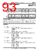
92 / 440 page  SDRAM Controller Registers 7-4 Élan™SC520 Microcontroller Register Set Manual SDRAM Timing Control (DRCTMCTL) Memory-Mapped MMCR Offset 12h Register Description This register controls the SDRAM device timing. Note: A programmable reset preserves this register’s state. See the PRG_RST_ENB bit description on page 3-3. Bit Definitions Programming Notes This register (DRCTMCTL) should be modified only when the write buffer and the read-ahead feature of the read buffer are disabled in the DBCTL register (see page 8-3). 7 6 5 4 3 2 1 0 Bit Reserved CAS_LAT RAS_PCHG_DLY[1–0] RAS_CAS_DLY[1–0] Reset 00011010 R/W RSV R/W R/W R/W Bit Name Function 7 –5 Reserved Reserved This bit field should be written to 0 for normal system operation. 4 CAS_LAT SDRAM CAS Latency This bit controls the SCASx signal latency timing to all the SDRAM banks. 0 = Cycle latency is 2T. 1 = Cycle latency is 3T (default). Where T is 15 ns (one half of the 33-MHz clock cycle). To make the CAS_LAT bit setting take effect, a Load Mode Register command must be issued to the SDRAM devices via the OPMODE_SEL bit field of the DRCCTL register (see page 7-3). Incorrect operation can occur if the CAS_LAT bit is modified and the Load Mode Register command is not issued to the SDRAM devices. 3 –2 RAS_PCHG_ DLY[1–0] SDRAM RAS Precharge Delay This bit field determines the SRASx signal precharge delay. 00 = 2T 01 = 3T 10 = 4T (default) 11 = 6T Where T is 15 ns (one half of the 33-MHz clock cycle). 1 –0 RAS_CAS_ DLY[1–0] SDRAM RAS-to-CAS Delay This bit field determines the SRASx-to-SCASx delay. 00 = 2T 01 = 3T 10 = 4T (default) 11 = Reserved Where T is 15 ns (one half of the 33-MHz clock cycle). |
|
Link URL |
| Does ALLDATASHEET help your business so far? [ DONATE ] |
About Alldatasheet | Advertisement | Contact us | Privacy Policy | Link to Datasheet | Link Exchange | Manufacturer List All Rights Reserved©Alldatasheet.com |
| Russian : Alldatasheetru.com | Korean : Alldatasheet.co.kr | Spanish : Alldatasheet.es | French : Alldatasheet.fr | Italian : Alldatasheetit.com Portuguese : Alldatasheetpt.com | Polish : Alldatasheet.pl | Vietnamese : Alldatasheet.vn Indian : Alldatasheet.in | Mexican : Alldatasheet.com.mx | British : Alldatasheet.co.uk | New Zealand : Alldatasheet.co.nz |
|
Family Site : ic2ic.com |
icmetro.com |
 New Zealand ▼
 English
 Chinese
 German
 Japanese
 Russian
 Korean
 Spanish
 French
 Italian
 Portuguese
 Polish
 Vietnamese
 Indian
 Mexican
 British
 New Zealand