|
Electronic Components Datasheet Search |
|
|
Electronic Components Datasheet Search |
|
ELANSC520 Datasheet(PDF) 96 Page - Advanced Micro Devices |
|
|
|||||||||||||||||||||||||||||
ELANSC520 Datasheet(HTML) 96 Page - Advanced Micro Devices |
|
|
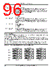
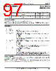
96 / 440 page  SDRAM Controller Registers 7-8 Élan™SC520 Microcontroller Register Set Manual Programming Notes This register (DRCBENDADR) should be modified only when the write buffer and the read-ahead feature of the read buffer are disabled in the DBCTL register (see page 8-3). The value specified in each BNKx_END bit field determines the upper address boundary of the corresponding SDRAM bank in 4Mbyte increments. Each bank’s lower boundary is determined by the end of the next-lower enabled bank, so the addressable SDRAM space is the concatenation of the enabled banks. The top of the highest configured bank is the top of memory. If any particular bank is disabled (via its BNKx_ENB bit), the associated BNKx_END bit field value has no effect. Banks do not have to be enabled contiguously. Figure 7-1 gives a few examples of SDRAM bank configuration. Figure 7-1 Examples of Bank Ending Address Configuration 22 –16 BNK2_END [28 –22] Bank 2 Ending Address This bit field determines the Bank 2 boundary, defined in 4-Mbyte increments. This value is compared to physical address bits 28 –22 during an SDRAM request to select a bank. Bank 2 is selected if physical address bits 28–22 are less than the BNK2_END bit field value but greater than or equal to the value specified by the BNK1_END bit field (or the next lower enabled bank’s end value if Bank 1 is disabled. 15 BNK1_ENB Bank 1 Enable This bit enables Bank 1. 0 = Disabled 1 = Enabled 14 –8 BNK1_END [28 –22] Bank 1 Ending Address This bit field determines the Bank 1 boundary, defined in 4-Mbyte increments. This value is compared to physical address bits 28 –22 during an SDRAM request to select a bank. Bank 1 is selected if physical address bits 28–22 are less than the BNK1_END bit field value but greater than or equal to the value specified by the BNK0_END bit field (or 0 if Bank 0 is disabled). 7 BNK0_ENB Bank 0 Enable This bit enables Bank 0. 0 = Disabled 1 = Enabled 6 –0 BNK0_END [28 –22] Bank 0 Ending Address This bit field determines the Bank 0 boundary, defined in 4-Mbyte increments. This value is compared to physical address bits 28 –22 during an SDRAM request to select a bank. Bank 0 is selected if physical address bits 28–22 are less than the BNK0_END bit field value. Bit Name Function Bank 0 Bank 1 Bank 2 Bank 3 Example 1 Total 32 Mbytes Example 2 56 Mbytes Example 3 192 Mbytes BNK0_END = 02h 7FFFFFh (8 Mbytes) 000000h BNK1_END = 04h FFFFFFh (8 Mbytes) 800000h BNK2_END = 06h 17FFFFFh (8 Mbytes) 1000000h BNK3_END = 08h 1FFFFFFh (8 Mbytes) 1800000h BNK0_END = 08h 1FFFFFFh (32 Mbytes) 0000000h BNK1_END = 10h 3FFFFFFh (32 Mbytes) 2000000h BNK2_END = 20h 7FFFFFFh (64 Mbytes) 4000000h BNK3_END = 30h BFFFFFFh (64 Mbytes) 8000000h BNK0_END = 04h FFFFFFh (16 Mbytes) 000000h BNK1_END = 06h 17FFFFFh (8 Mbytes) 1000000h BNK2_END = “Don’t Care” Disabled (BNK2_ENB = 0) BNK3_END = 0Eh 37FFFFFh (32 Mbytes) 1800000h |
|
Link URL |
| Does ALLDATASHEET help your business so far? [ DONATE ] |
About Alldatasheet | Advertisement | Contact us | Privacy Policy | Link to Datasheet | Link Exchange | Manufacturer List All Rights Reserved©Alldatasheet.com |
| Russian : Alldatasheetru.com | Korean : Alldatasheet.co.kr | Spanish : Alldatasheet.es | French : Alldatasheet.fr | Italian : Alldatasheetit.com Portuguese : Alldatasheetpt.com | Polish : Alldatasheet.pl | Vietnamese : Alldatasheet.vn Indian : Alldatasheet.in | Mexican : Alldatasheet.com.mx | British : Alldatasheet.co.uk | New Zealand : Alldatasheet.co.nz |
|
Family Site : ic2ic.com |
icmetro.com |
 New Zealand ▼
 English
 Chinese
 German
 Japanese
 Russian
 Korean
 Spanish
 French
 Italian
 Portuguese
 Polish
 Vietnamese
 Indian
 Mexican
 British
 New Zealand