|
Electronic Components Datasheet Search |
|
|
Electronic Components Datasheet Search |
|
ELANSC520 Datasheet(PDF) 85 Page - Advanced Micro Devices |
|
|
|||||||||||||||||||||||||||||
ELANSC520 Datasheet(HTML) 85 Page - Advanced Micro Devices |
|
|
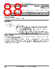
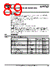
85 / 440 page  PCI Bus Host Bridge Registers Élan™SC520 Microcontroller Register Set Manual 6-21 Programming Notes This register is reset by a system reset or by a PCI bus reset. A PCI bus reset is initiated by setting the PCI_RST bit in the HBCTL register (see page 6-3). This register (PCISTACMD) is register number 1 in the host bridge-specific PCI configuration space. The PCI Local Bus Specification, Revision 2.2, defines four bit fields in the Status/Command register that are reserved in the ÉlanSC520 microcontroller. These PCI bus functions do not apply to the host bridge controller: s Wait cycle control (bit 7): the host bridge controller does not support address/data stepping. s VGA palette snoop enable (bit 5): the host bridge is not a graphics device. s Memory write and invalidate enable (bit 4): the host bridge does not generate memory write and invalidate commands as a PCI bus master. s Special cycle recognition (bit 3): the host bridge ignores PCI bus special cycles. 6 PERR_RES Parity Error Response This bit controls the host bridge’s response to parity errors. 0 = The host bridge master and target controllers ignore parity errors. The host bridge treats transactions that have a parity error (address or data) as normal transactions. In other words, it behaves as if nothing is wrong. The D_PERR_DET bit (see page 6-20) is not set for data parity errors, and a target abort is not issued for address parity errors. 1 = The host bridge master and target controllers report parity errors. The host bridge responds to data parity errors by setting the D_PERR_DET bit. The host bridge target controller responds to address parity errors by terminating the transaction with a target abort. The PERR_RES bit must not be changed except during PCI bus initialization after a system reset. See the Élan™SC520 Microcontroller User’s Manual, order #22004, for information about PCI bus initialization. 5 –3 Reserved Reserved This bit field should be written to 0 for normal system operation. 2BUS_MAS Master Enable This enables the host bridge master controller to generate cycles on the PCI bus. 1 = The host bridge master controller is always enabled. This bit is internally fixed to 1. 1MEM_ENB Memory Access Enable This bit enables the host bridge target controller to respond to PCI bus master memory cycles. 0 = The host bridge target controller is disabled. 1 = The host bridge target controller is enabled to respond to PCI bus master memory cycles. The MEM_ENB bit must not be changed except during PCI bus initialization after a system reset. See the Élan™SC520 Microcontroller User’s Manual, order #22004, for information about PCI bus initialization. 0IO_ENB I/O Space Enable This bit is normally used to enable the host bridge target controller to respond to PCI bus master I/O cycles, however the ÉlanSC520 microcontroller host bridge ignores all I/O cycles from PCI bus masters. 0 = The host bridge does not respond to PCI bus I/O cycles. This bit is internally fixed to 0. Bit Name Function |
|
Link URL |
| Does ALLDATASHEET help your business so far? [ DONATE ] |
About Alldatasheet | Advertisement | Contact us | Privacy Policy | Link to Datasheet | Link Exchange | Manufacturer List All Rights Reserved©Alldatasheet.com |
| Russian : Alldatasheetru.com | Korean : Alldatasheet.co.kr | Spanish : Alldatasheet.es | French : Alldatasheet.fr | Italian : Alldatasheetit.com Portuguese : Alldatasheetpt.com | Polish : Alldatasheet.pl | Vietnamese : Alldatasheet.vn Indian : Alldatasheet.in | Mexican : Alldatasheet.com.mx | British : Alldatasheet.co.uk | New Zealand : Alldatasheet.co.nz |
|
Family Site : ic2ic.com |
icmetro.com |
 New Zealand ▼
 English
 Chinese
 German
 Japanese
 Russian
 Korean
 Spanish
 French
 Italian
 Portuguese
 Polish
 Vietnamese
 Indian
 Mexican
 British
 New Zealand