|
Electronic Components Datasheet Search |
|
|
Electronic Components Datasheet Search |
|
ELANSC520 Datasheet(PDF) 80 Page - Advanced Micro Devices |
|
|
|||||||||||||||||||||||||||||
ELANSC520 Datasheet(HTML) 80 Page - Advanced Micro Devices |
|
|
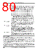
80 / 440 page  PCI Bus Host Bridge Registers 6-16 Élan™SC520 Microcontroller Register Set Manual Programming Notes After this register (PCICFGADR) is written with the requisite information, an access must be made to the PCICFGDATA register (see page 6-17) to cause the PCI bus configuration cycle to occur on the PCI bus. This register is reset by a system reset. The bits in this register are not affected by a PCI bus reset. A PCI bus reset is initiated by setting the PCI_RST bit in the HBCTL register (see page 6-3). This register must be accessed as a doubleword. Accesses that are less than a doubleword in width are treated as normal PCI bus I/O or (if so mapped) GP bus I/O accesses. No configuration cycles are generated if the access is not to the entire doubleword. In the ÉlanSC520 microcontroller, the doubleword starting at 0CF8h must not be mapped to the GP bus. The ÉlanSC520 microcontroller does not generate special cycles. In other words, setting the BUS_NUM bit field to 00h, the DEVICE_NUM bit field to 11111b, the FUNCTION_NUM bit field to 111b, and the REGISTER_NUM field to 00000b does not generate a special cycle. Instead, this setup generates a PCI bus configuration write cycle. 15–11 DEVICE_NUM [4–0] Device Number This bit field specifies the device to address on the bus that is specified by the BUS_NUM bit field. For type zero configuration cycles (if the BUS_NUM bit field is 00h), the DEVICE_NUM bit field value selects one of the following bit patterns to be driven on the PCI bus AD31–AD11 pins during the address phase of the cycle: 00d = Address the ÉlanSC520 microcontroller’s host bridge (if the BUS_NUM bit field is 00h). The cycle is not visible on the PCI bus. (I.e., no bit pattern is driven externally.) 01d = The AD12 pin is driven High, and the other pins of AD31–AD11 are driven Low. 02d = The AD13 pin is driven High, and the other pins of AD31–AD11 are driven Low. 03d = The AD14 pin is driven High, and the other pins of AD31–AD11 are driven Low. . . . . . 19d = The AD30 pin is driven High, and the other pins of AD31–AD11 are driven Low. 20d = The AD31 pin is driven High, and the other pins of AD31–AD11 are driven Low. 21–31d = All pins AD31–AD11 are driven Low (to 0); but the host bridge does not accept configuration accesses using these DEVICE_NUM bit field values, so configuration reads or writes with these values result in a Master Abort. Performing a configuration read with these values returns FFFFh in the data. In a typical system design, one of the address pins AD31–AD12 is resistively coupled to each PCI bus device’s IDSEL input, so a DEVICE_NUM bit field value in the range 1–20d selects the corresponding PCI bus device during a type zero configuration cycle. For type one configuration cycles (if the BUS_NUM bit field is not 00h), the contents of this bit field are driven unchanged on the PCI bus during the address phase of the cycle. 10–8 FUNCTION_ NUM[2 –0] Function Number This bit field specifies the function number within the device specified by the DEVICE_NUM bit field. For host bridge configuration cycles (if the BUS_NUM and DEVICE_NUM bit fields are both 0), the function number is ignored because the host bridge is a single-function device. For all other configuration cycles (type zero or type one), the contents of this bit field are driven unchanged on the PCI bus during the address phase of the configuration cycle. 7–2 REGISTER_ NUM[5 –0] Register Number This bit field specifies the register number within the function specified by the FUNCTION_NUM bit field. For host bridge configuration cycles (if the BUS_NUM and DEVICE_NUM bit fields are both 0), the REGISTER_NUM bit field is used to address the host bridge PCI-indexed registers (see the descriptions beginning on page 6-18). REGISTER_NUM bits 5–0 are used as bits 7–2 of the PCI index address to address doublewords in the configuration space. Byte locations within a doubleword are addressed by accessing the corresponding bytes of the PCICFGDATA register (see page 6-17). For all other configuration cycles (type zero or type one), the contents of this bit field are driven unchanged on the PCI bus during the address phase of the configuration cycle. 1–0 Reserved Reserved This bit field is ignored during writes to this register. It always returns 0 when read. During the address phase of a configuration cycle, address pins AD1–AD0 are driven to 00b to indicate a type zero configuration cycle, or to 01b to indicate a type one configuration cycle, depending on value of the BUS_NUM bit field. Bit Name Function |
|
Link URL |
| Does ALLDATASHEET help your business so far? [ DONATE ] |
About Alldatasheet | Advertisement | Contact us | Privacy Policy | Link to Datasheet | Link Exchange | Manufacturer List All Rights Reserved©Alldatasheet.com |
| Russian : Alldatasheetru.com | Korean : Alldatasheet.co.kr | Spanish : Alldatasheet.es | French : Alldatasheet.fr | Italian : Alldatasheetit.com Portuguese : Alldatasheetpt.com | Polish : Alldatasheet.pl | Vietnamese : Alldatasheet.vn Indian : Alldatasheet.in | Mexican : Alldatasheet.com.mx | British : Alldatasheet.co.uk | New Zealand : Alldatasheet.co.nz |
|
Family Site : ic2ic.com |
icmetro.com |
 New Zealand ▼
 English
 Chinese
 German
 Japanese
 Russian
 Korean
 Spanish
 French
 Italian
 Portuguese
 Polish
 Vietnamese
 Indian
 Mexican
 British
 New Zealand