|
Electronic Components Datasheet Search |
|
|
Electronic Components Datasheet Search |
|
ELANSC520 Datasheet(PDF) 90 Page - Advanced Micro Devices |
|
|
|||||||||||||||||||||||||||||
ELANSC520 Datasheet(HTML) 90 Page - Advanced Micro Devices |
|
|
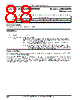
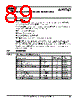
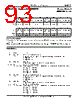
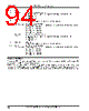
90 / 440 page  SDRAM Controller Registers 7-2 Élan™SC520 Microcontroller Register Set Manual SDRAM Control (DRCCTL) Memory-Mapped MMCR Offset 10h Register Description This register controls various features of the SDRAM controller. Note: A programmable reset preserves this register’s state. See the PRG_RST_ENB bit description on page 3-3. Bit Definitions 7 6 5 4 3 2 1 0 Bit WB_TST_ ENB Reserved RFSH_SPD[1–0] RFSH_ENB OPMODE_SEL[2–0] Reset 00010000 R/W R/W! RES R/W R/W R/W Bit Name Function 7 WB_TST_ ENB Write Buffer Test Mode Enable This bit selects the source of the debugging information available on the three system test pins. 0 = Write buffer test mode is disabled. (System test mode.) The three system test pins function as CF_DRAM, DATASTRB and CF_ROM_GPCS pins. 1 = Write buffer test mode is enabled. The three system test pins function as WBMSTR2 – WBMSTR0 for write buffer master trace purposes. If the write buffer is enabled (WB_ENB is set in the DBCTL register, see page 8-3), the WBMSTR2 –WBMSTR0 signals provide write buffer master trace information during write cycles from the write buffer to SDRAM. Master trace information specifies which masters contributed to the level (rank) that is currently being written to SDRAM from the write buffer. Contributing masters can be one or more of: Am5x86 CPU, PCI, or GP bus DMA. If the write buffer is disabled, or during read cycles if the write buffer is enabled, the WBMSTR2 –WBMSTR0 signals reflect the master that is currently requesting SDRAM access. Software writes to this bit are ignored when the AMDebug™ technology mode is active. This ensures that microcontroller software cannot remove control of the pins from the software driving the AMDebug technology port. If AMDebug technology mode is not active, software can write to this bit. Refer to the Élan™SC520 Microcontroller User’s Manual, order #22004, for more information about system test mode and write buffer test mode. 6 Reserved Reserved This bit field should be written to 0 for normal system operation. 5 –4 RFSH_SPD [1–0] SDRAM Refresh Request Speed These two bits determine the SDRAM refresh request rate. 00 = 7.8 ms 01 = 15.6 ms (default) 10 = 31.2 ms 11 = 62.5 ms 3 RFSH_ENB Refresh Enable 0 = SDRAM refresh is disabled. This mode should be used for SDRAM detection and sizing algorithms. Disabling SDRAM refresh should not be done in normal operation. 1 = SDRAM refresh is enabled. Note: Refresh cycles are not generated to SDRAM banks that are not enabled via the BNKx_ENB bits in the DRCBENDADR register (see page 7-7). |
|
Link URL |
| Does ALLDATASHEET help your business so far? [ DONATE ] |
About Alldatasheet | Advertisement | Contact us | Privacy Policy | Link to Datasheet | Link Exchange | Manufacturer List All Rights Reserved©Alldatasheet.com |
| Russian : Alldatasheetru.com | Korean : Alldatasheet.co.kr | Spanish : Alldatasheet.es | French : Alldatasheet.fr | Italian : Alldatasheetit.com Portuguese : Alldatasheetpt.com | Polish : Alldatasheet.pl | Vietnamese : Alldatasheet.vn Indian : Alldatasheet.in | Mexican : Alldatasheet.com.mx | British : Alldatasheet.co.uk | New Zealand : Alldatasheet.co.nz |
|
Family Site : ic2ic.com |
icmetro.com |
 New Zealand ▼
 English
 Chinese
 German
 Japanese
 Russian
 Korean
 Spanish
 French
 Italian
 Portuguese
 Polish
 Vietnamese
 Indian
 Mexican
 British
 New Zealand