|
Electronic Components Datasheet Search |
|
|
Electronic Components Datasheet Search |
|
ELANSC520 Datasheet(PDF) 39 Page - Advanced Micro Devices |
|
|
|||||||||||||||||||||||||||||
ELANSC520 Datasheet(HTML) 39 Page - Advanced Micro Devices |
|
|
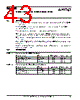
39 / 440 page  System Address Mapping Registers Élan™SC520 Microcontroller Register Set Manual 2-7 28 –26 ATTR[2 –0] Attribute If the TARGET bit field selects the PCI bus (for PAR0 and PAR1 only), this bit field (ATTR) is ignored. If the TARGET bit field selects GP bus I/O or memory, this bit field (ATTR) specifies the GP bus chip select that is targeted, as follows: 000 = GPCS0 001 = GPCS1 010 = GPCS2 011 = GPCS3 100 = GPCS4 101 = GPCS5 110 = GPCS6 111 = GPCS7 If the TARGET bit field selects SDRAM or one of the ROM/Flash chip selects, each bit in this bit field (ATTR) specifies an attribute. The attribute bits for the region can be set or cleared independently, with the following effect: 0xx = Code execution is allowed in programmed memory region. 1xx = Code execution is prevented in programmed memory region. An attempt to execute code results in a processor exception and returns an illegal operand code (FFFFh). This attribute is useful for debugging software; for example, to prevent a program from erroneously executing out of a data region. x0x = Caching is enabled for the programmed memory region (Am5x86 CPU cache). x1x = Caching is disabled for the programmed memory region. This attribute can be used to minimize cache write-back cycle overhead in regions that are shared between the Am5x86 CPU and PCI bus masters or GP bus DMA devices. Software must flush the cache immediately after setting this attribute. xx0 = Writes are enabled in the programmed memory region. xx1 = Write protection is enabled (writes are disabled) in the programmed memory region. Write protection prevents writes from occurring in the region’s address range. Write- protect violations are reported by the WPVSTA register (see page 2-4), and a corresponding interrupt can be enabled via the WPV_INT_ENB bit in the ADDDECCTL register (see page 2-2). 25 PG_SZ Page Size This bit selects the page size of the memory region defined by the SZ_ST_ADR bit field. This bit is ignored during I/O cycles. 0 = 4-Kbyte page size selected 1 = 64-Kbyte page size selected Each PARx window’s total size in memory space is defined by the combined settings of the PG_SZ and SZ_ST_ADR bit fields. The PG_SZ bit value affects the window start address resolution, the window size resolution, and the total size that is possible for the window. Bit Name Function |
|
Link URL |
| Does ALLDATASHEET help your business so far? [ DONATE ] |
About Alldatasheet | Advertisement | Contact us | Privacy Policy | Link to Datasheet | Link Exchange | Manufacturer List All Rights Reserved©Alldatasheet.com |
| Russian : Alldatasheetru.com | Korean : Alldatasheet.co.kr | Spanish : Alldatasheet.es | French : Alldatasheet.fr | Italian : Alldatasheetit.com Portuguese : Alldatasheetpt.com | Polish : Alldatasheet.pl | Vietnamese : Alldatasheet.vn Indian : Alldatasheet.in | Mexican : Alldatasheet.com.mx | British : Alldatasheet.co.uk | New Zealand : Alldatasheet.co.nz |
|
Family Site : ic2ic.com |
icmetro.com |
 New Zealand ▼
 English
 Chinese
 German
 Japanese
 Russian
 Korean
 Spanish
 French
 Italian
 Portuguese
 Polish
 Vietnamese
 Indian
 Mexican
 British
 New Zealand