|
Electronic Components Datasheet Search |
|
|
Electronic Components Datasheet Search |
|
ELANSC520 Datasheet(PDF) 81 Page - Advanced Micro Devices |
|
|
|||||||||||||||||||||||||||||
ELANSC520 Datasheet(HTML) 81 Page - Advanced Micro Devices |
|
|
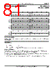
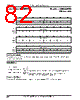
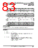
81 / 440 page  PCI Bus Host Bridge Registers Élan™SC520 Microcontroller Register Set Manual 6-17 PCI Configuration Data (PCICFGDATA) Direct-Mapped I/O Address 0CFCh Register Description Software reads or writes this register to initiate a PCI bus configuration cycle after setting up the PCICFGADR register (see page 6-15). Bit Definitions Programming Notes The ENABLE bit must be set in the PCICFGADR register for an access to this register (PCICFGDATA) to result in a PCI bus configuration cycle. Otherwise the cycle accesses the PCI bus I/O space. This register can be accessed as a doubleword, word, or byte. The appropriate CBEx signal combinations are driven on the PCI bus during the data phase of the configuration cycle. In the ÉlanSC520 microcontroller, the doubleword starting at 0CFCh must not be mapped to the GP bus. 31 30 29 28 27 26 25 24 Bit CFG_DATA[31–24] Reset xxxxxxxx R/W R/W 23 22 21 20 19 18 17 16 Bit CFG_DATA[23–16] Reset xxxxxxxx R/W R/W 15 14 13 12 11 10 9 8 Bit CFG_DATA[15–8] Reset xxxxxxxx R/W R/W 7 6 5 4 3 2 1 0 Bit CFG_DATA[7–0] Reset xxxxxxxx R/W R/W Bit Name Function 31–0 CFG_DATA [31–0] Configuration Data This bit field contains the data for the configuration access cycle (read or write). |
|
Link URL |
| Does ALLDATASHEET help your business so far? [ DONATE ] |
About Alldatasheet | Advertisement | Contact us | Privacy Policy | Link to Datasheet | Link Exchange | Manufacturer List All Rights Reserved©Alldatasheet.com |
| Russian : Alldatasheetru.com | Korean : Alldatasheet.co.kr | Spanish : Alldatasheet.es | French : Alldatasheet.fr | Italian : Alldatasheetit.com Portuguese : Alldatasheetpt.com | Polish : Alldatasheet.pl | Vietnamese : Alldatasheet.vn Indian : Alldatasheet.in | Mexican : Alldatasheet.com.mx | British : Alldatasheet.co.uk | New Zealand : Alldatasheet.co.nz |
|
Family Site : ic2ic.com |
icmetro.com |
 New Zealand ▼
 English
 Chinese
 German
 Japanese
 Russian
 Korean
 Spanish
 French
 Italian
 Portuguese
 Polish
 Vietnamese
 Indian
 Mexican
 British
 New Zealand